electronics-journal.com
14
'22
Written on Modified on
World’s First Current Sensing Technology From Toshiba, Implemented in GaN Devices Enables Lower Power Loss, Higher Accuracy Current Sensing, and Smaller Power Supply Systems
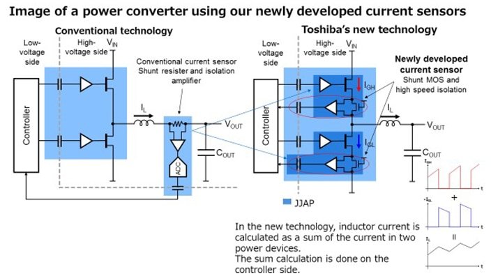
Toshiba Electronic Devices & Storage Corporation (“Toshiba”) has developed the world’s first[1] integrated shunt MOS current sensor in a half bridge (HB) module.

The sensor enables power electronics systems to monitor current with high accuracy, but with no increase in power loss, when used on devices such as gallium nitride (GaN) power devices, and will contribute to size reductions in those systems and electronic equipment.
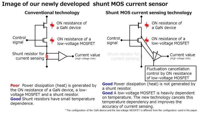
Global promotion of carbon neutrality requires more efficient electronic equipment, especially smaller-sized systems. However, integrating HB modules and current sensors on a chip has proved difficult as they must be located on both sides of inductors. Efforts to reduce power dissipation (heat) lowers the accuracy of current sensing, as it relies on shunt resistors. Today’s technology can realize high accuracy current sensors, but not lower loss.
Toshiba’s new technology utilizes a cascode comprising a low voltage MOSFET (metal oxide semiconductor field effect transistor) connected to a GaN field effect transistor[2] for current sensing, eliminating the shunt resistor and its power dissipation. Performance and measuring accuracy are also enhanced by circuit optimization and cutting-edge calibration technology that secures a bandwidth of over 10MHz. Integrated into an HB module, the new IC improves switching frequency, reduces the size of capacitors and inductors, and contributes to smaller electronic equipment.
Power semiconductors that improve power converter efficiency, are a key focus area for Toshiba, including GaN devices. Toshiba will contribute to the realization of carbon neutrality by advancing the early integration of this new technology into power semiconductors and securing an early market launch.

Details of these new technology are introduced in a paper published on the Japanese Journal of Applied Physics (JJAP) website.
URL:https://iopscience.iop.org/article/10.35848/1347-4065/ac4446
Toshiba announced related technology at the 2021 International Conference on Solid State Devices & Materials (SSDM), an international conference held in September, 2021.
Notes
[1] As of January 2022, Toshiba research
[2] A configuration to realize normally off GaN devices combining normally on GaN devices and low-voltage MOSFETs
* Company names, product names, and service names may be trademarks of their respective companies.
* Information in this document, including product prices and specifications, content of services and contact information, is current on the date of the announcement but is subject to change without prior notice.
www.toshiba.com

