
Toshiba Adds Five New MOSFET Gate Driver ICs that Will Help Reduce Device Footprints
Toshiba Electronic Devices & Storage Corporation ("Toshiba") has added five products to its lineup of MOSFET gate driver ICs in the TCK42xG Series for mobile devices such as wearables. The new products in the series are equipped with an overvoltage lockout function and control the gate voltage of an external MOSFET according to the input voltage.

TCK42xG Series supports external back-to-back MOSFETs.
The new products are: “TCK420G” for 24V power lines; “TCK422G” and “TCK423G” for 12V power lines; “TCK424G” for 9V power lines; and “TCK425G” for 5V power lines. Along with the already launched “TCK421G” for 20V power lines, they are available now.
With this addition, TCK42xG series now allow users to select a gate-source voltage from two types, 10V and 5.6V, offering coverage of more MOSFETs. In addition, the lineup of the different detection voltages for the input overvoltage lockout function allows the products to be used for power lines from 5V to 24V. When combined with an external back-to-back MOSFET, they are also suitable for configuring a load switch circuit (Fig.1) or a power multiplexer circuit (Fig.2). with a reverse current blocking function. Furthermore, with their built-in charge pump circuit supporting a wide range of input voltages, from 2.7V to 28V, they provide stable voltage between the gate and source of an external back-to-back MOSFET with intermittent operation. This allows large currents to be switched.
Housed in a WCSP6G[1] package, one of the smallest in the industry[2], the TCK42xG series realizes high density mounting for small devices, such as wearables and smartphones, helping to reduce their footprint.
Toshiba has also developed “Power multiplexer circuit” Reference Design, a reference design example for a power multiplexer that utilizes the functions of TCK42xG. It is available on Toshiba’s website from today.
Notes :
[1] A 1.2mm × 0.8mm chip scale package
[2] Among MOSFET gate driver ICs, Toshiba survey as of June 2022.
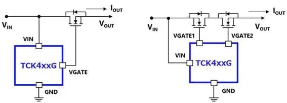
Fig.1: Load switch circuit (Single High-side, Back-to-Back)
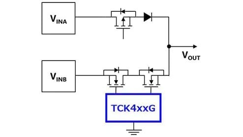
Fig.2: Power multiplexer circuit
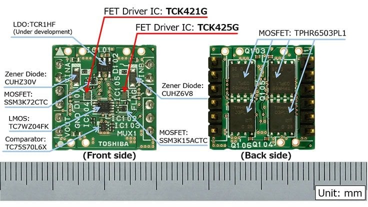
Fig.3: Power multiplexer circuit board
Applications
- Wearables
- Smartphones
- Notebook PC, tablets
- Storage equipment, etc.
Features
- Gate-source voltage setting (5.6V, 10V) depending on input voltage with a built-in charge pump circuit
- Over voltage lock out supports 5V to 24V
- Low input OFF current: IQ (OFF) = 0.5μA (max) @VIN=5V
