Toshiba’s young engineers: The ability to listen and think drives innovation
Remote work has become the new normal due to the COVID-19 pandemic. Some people use the time freed up from commuting to enrich their private lives, while others use it to study, as an investment in their future selves.
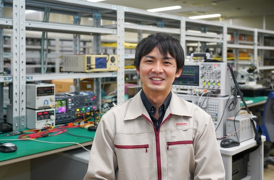
- The appeal of working on manufacturing from upstream to downstream: information needed can be found in-house.
- The pressure of being entrusted with tasks helped one young engineer to grow.
- What change in mindset was key to Toshiba's development of a new generation of HDDs?
The engineer featured in this article said he used the time gained during the COVID-19 pandemic to achieve his long-held goal of getting a motorcycle license. While enjoying riding along the quiet coastline, avoiding crowds, he says that when he looks at the scenery at his destination he thinks about the ideas sparked by the many conversations and new insights he has gained from the numerous engineers around him
The joy of designing for yourself
Toshiba Group manufactures products in many fields, exemplified by turbines for power generation in the energy sector, railroad equipment, lighting, semiconductors, hard disk drives (HDDs). One of the Group’s characteristics is that it often handles the entire production process from design to manufacture. Yuki Kawamitsu of Toshiba Electronic Devices & Storage Corporation, who works on HDD development, says he joined the company after he found Toshiba’s manufacturing system appealing.
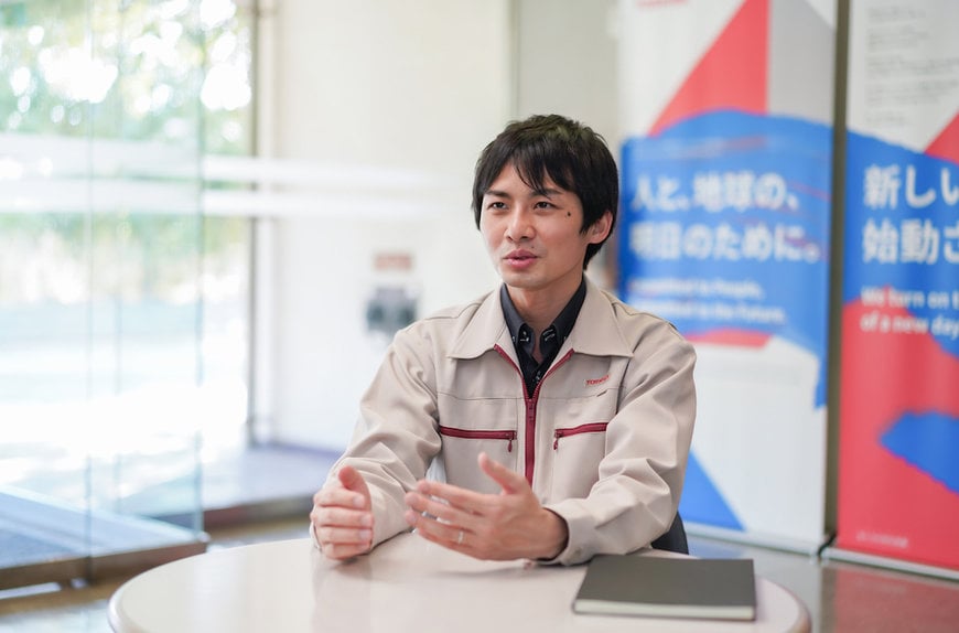
Yuki Kawamitsu, PCB&LSI Engineering Group, Common Core Engineering Dept., Storage Products Design & Production Div., Toshiba Electronic Devices & Storage Corporation
“Toshiba is one of the only Japanese companies to does in-house computer aided design (CAD) for the circuit design of printed circuit board (PCB) for HDDs. For people like me, who love manufacturing, the ability to do the design yourself is the ultimate joy.”
Many companies outsource process, for reasons including cutting costs. However, the fact that each process of design and manufacturing is conducted within the Group encourages knowledge exchanges and synergy, which has led to numerous innovations at Toshiba. The knowledge accumulated within the Group now supports Toshiba’s technological capabilities and contributes to solving social issues.
Kawamitsu says there are many other advantages to working as an engineer at Toshiba besides being involved in the entire manufacturing process from upstream to downstream. One is exchanges within the Group.
“When the parts we use are manufactured by Toshiba Group companies, we can talk directly with the engineers who made them, and get more in-depth information than when we introduce products from other companies. Since we’re all Toshiba engineers, everyone is friendly and willing to talk. Much of this information contains tips for growing as an engineer that are difficult to come up with on your own. I actually feel that my knowledge of components and technological development is deepening and my own circuit design skills are improving.”
Being entrusted with a task drives growth as an engineer
Kawamitsu majored in electromagnetic compatibility at university. He studied the impact of electromagnetic waves emitted by industrial products on the environment, and researched ways to reduce electromagnetic waves by improving the wiring of PCBs and other means. Around half a year after joining the company, he was entrusted with his first major task; to solve the issue of electromagnetic wave noise in PCBs. Although this was close to what he had been studied at university, he said he was surprised at his supervisor telling him, “I’ll leave it to you, so go ahead and do what you want while studying,” and at the expectations and open-mindedness that were implied.
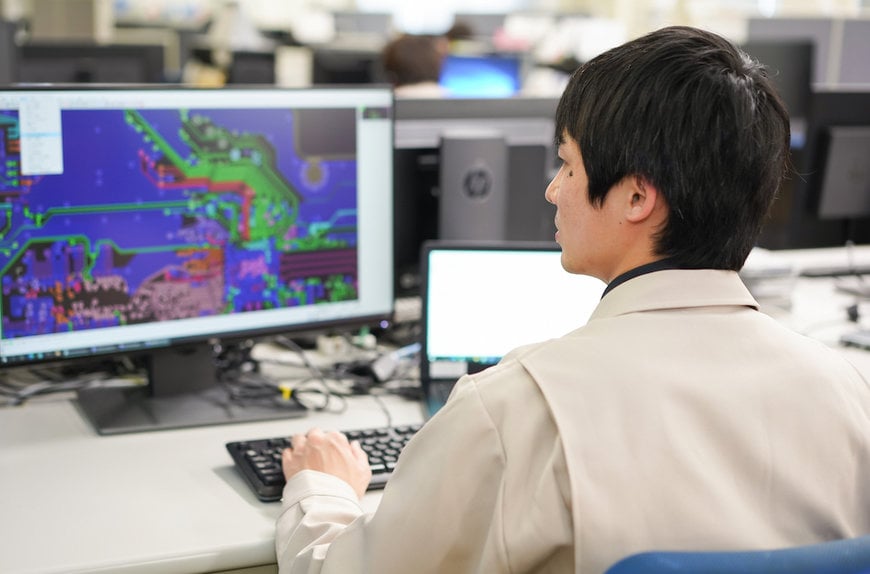
He says that learning about the efforts of engineers through glimpses of past product designs is both a source of enjoyment and food for growth
“We evaluate problematic PCBs to identify the problems and propose solutions, then incorporate them into the CAD design and re-evaluate the completed PCBs. I was allowed to do all of these processes, right from creating schedules, by myself.
“While it was a very challenging job, I asked around in the company for solutions to things I didn’t understand. Thanks to this, I was able to learn who does what work and what kind of communication I should take. Above all, I believe I took my first step as a professional engineer.”
This is a clear representation of Toshiba’s manufacturing. Toshiba is not a hierarchical company, but rather a company of equals, drawing on each other’s expertise to create products. There is respect for the knowledge of others, regardless of age, and, at the same time, pride in one’s own expertise. It’s thanks to working in this environment that Kawamitsu was able to grow so fast.
How a change in thinking resulted in next-generation HDDs
The high-capacity HDDs for data centers that Kawamitsu’s group is working on are one of the most important devices in modern society, where information is the most valuable resource. Because the required performance constantly increases, it is also an area where development cannot be allowed to slow down.
“Size formats are fixed. The key is how large of a storage capacity can be achieved. Manufacturers around the world compete on this basis.”
In this competition to develop, the design of PCBs that Kawamitsu designs play an important role. The capacity of an HDD is determined by the way data is recorded on a rotating disk and how many of these disks can be fitted into the casing. To achieve this, an internal structure that makes non-disk components smaller must be devised. However, it’s always difficult to do this. What’s more, Kawamitsu was aiming for a size reduction of 50% over the previous generation’s products.
“The semiconductors and other components on the PCBs get smaller every year, but it’s still not enough. It is then important to design patterns that determine how efficiently the components can be placed on the PCB.
“I got stuck designing PCBs so many times. I have to deal with PCBs that many more experienced engineers packed with the best technology a few years ago. I sometimes wonder what I could possibly do to improve on it.”
But this was where Kawamitsu, a self-titled “manufacturing enthusiast,” really came into his own. He wondered if it would be possible to shorten the wires connecting parts even if it was not possible to make the components themselves smaller. Kawamitsu set his sights on the grounds* that are placed in multiple areas on the PCB. Although the grounds were already purposely placed in different locations in order to efficiently install the necessary components, Kawamitsu boldly pursued this avenue.
*Ground: A location where the potential difference from the reference potential is 0 volts.
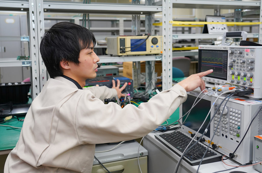
Kawamitsu says that it is important to believe that there is a solution to any problem and keep trying, and that this is one of the most exciting aspects of designing.
“In order to overcome the problems facing me, I thought it would be necessary to take a different approach to the engineer that made it. I reviewed the design with the primary goal of combining the ground wires that perform the same function into one. At this time, I was able to use the experience and viewpoints that I had cultivated in the jobs I had been entrusted with so far, and thought to myself, ‘if I take this wire, it will affect the other areas in this way.’”
This produced the remarkable result of significantly reducing the size of the printed circuit to 50% of that of the previous generation. The HDDs equipped with the PCBs created by Kawamitsu paved the way for Toshiba’s new generation of HDDs with even greater capacity. What are Kawamitsu, current thoughts, after achieving such a great result?
“At Toshiba, you can see the entire process of how a single product is made. The concepts, thoughts, and feelings of the engineers who make the components that go into the products also reach us. While absorbing such knowledge, I feel compelled to study areas other than my own in order to respond to their wishes. By doing this, I am able to meet colleagues with whom I can exchange ideas and improve my knowledge, because Toshiba Group encompasses a wide range of fields.
“I think that this is the best foundation for me to grow as an engineer. At Toshiba, which is responsible for all aspects of product development from upstream to downstream, we can proudly say, ‘we made this product,’ rather than ‘we made this part of the product.’”
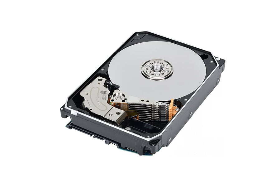
The latest product* features nine disks and 18TB of storage capacity with Flux Control Microwave-Assisted Magnetic Recording (FC-MAMR™) technology.
Note
- FC-MAMR™ is a trademark of Toshiba Electronic Devices & Storage Corporation.
- Other company names, product names, and service names mentioned herein may be trademarks of their respective companies.

