
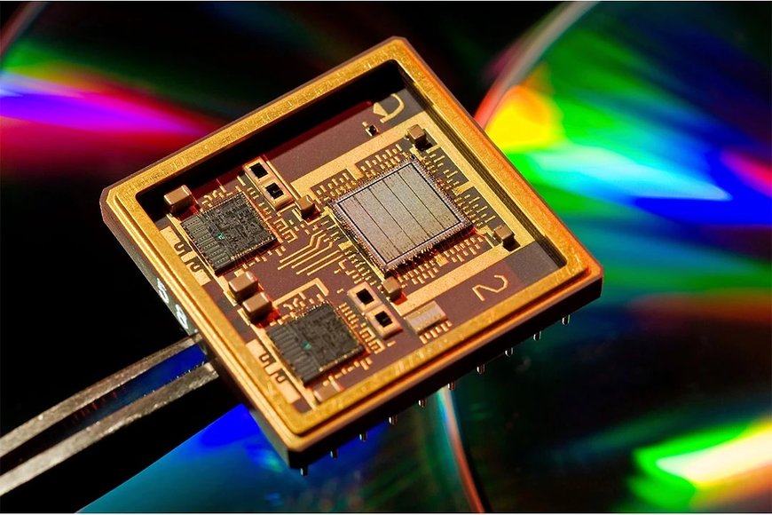
Ansys Multiphysics Solutions Achieve Certification for TSMC N4 Process and TSMC FINFLEX Architecture
Ansys is certified for TSMC’s innovative FINFLEX architecture on N3E for flexible power/performance tradeoffs.
TSMC’s FINFLEX™ architecture allows Ansys RedHawk-SC and Totem customers to make fine-grained speed-power tradeoffs, reducing a chip’s power footprint without sacrificing performance
- Ansys® Redhawk-SC™ and Ansys® Totem™ power integrity platforms are certified for TSMC’s FinFlex™ architecture on N3E
- The certification also extends to the TSMC N4 process technology
Ansys and TSMC continued their long-standing technology collaboration to announce certification of Ansys’ power integrity software for TSMC’s FINFLEX™ innovation as well as the TSMC N4 process. TSMC’s FINFLEX™ architecture allows Ansys RedHawk-SC and Totem customers to make fine-grained speed-power tradeoffs which reduce a chip’s power footprint without sacrificing performance. This is important for lowering the environmental impact of many semiconductor applications, including machine learning, 5G mobile, and high-performance computing (HPC). This latest collaboration builds on the recent certification of the Ansys platform for TSMC’s N3E process.
“The unparalleled flexibility of our FINFLEX™ innovation provides tremendous chip design advantage and flexibility to optimize for high performance, low power, or a balance between the two,” said Dan Kochpatcharin, head of Design Infrastructure Management Division at TSMC. “Our latest collaboration with Ansys on TSMC’s 3nm technology makes it easy for our mutual customers to take advantage of FINFLEX's benefits with full confidence in the power integrity and reliability signoff verification results from RedHawk-SC and Totem.”
Based on TSMC’s N3E process technology, TSMC FINFLEX architecture allows chip designers to choose from three options of FIN configurations for each standard cell implementation: One for highest performance and fastest clock frequencies, one for balanced efficient performance, and an ultra-power efficiency for the lowest leakage and highest density. This combination of characteristics enables chip designers to choose the best speed-performance option for each of the key functional blocks on a chip using the same design toolset.
"Ansys has developed an integrated software platform of multiphysics simulation and analysis tools with an emphasis on power management to minimize the design and operating costs of semiconductors," said John Lee, vice president and general manager of the electronics, semiconductor and optics business unit at Ansys. “Our ongoing collaboration with TSMC aligns with our efforts to enable a sustainable technology future, enabling mutual customers to improve chip performance while reducing power consumption."
www.ansys.com
