
electronics-journal.com
16
'26
Written on Modified on
Scaling Silicon Carbide Wafer Production for Digital Infrastructure
Infineon and Wolfspeed are transitioning to 200-millimeter substrates to improve semiconductor manufacturing efficiency for electric vehicles and data center power systems.
www.infineon.com
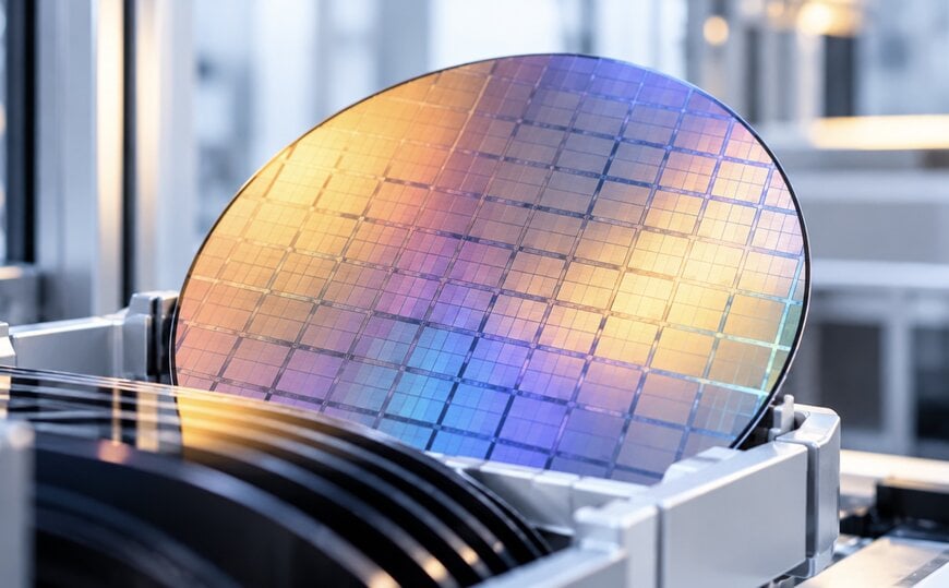
Semiconductor manufacturers Infineon Technologies and Wolfspeed have established a supply agreement to transition silicon carbide (SiC) wafer procurement from 150-millimeter to 200-millimeter substrates. This material upgrade supports the production of power semiconductors utilized in electric vehicle drivetrains, renewable energy systems, and digital infrastructure environments.
Addressing Power Conversion Challenges
The shift toward electrified transport and high-density computing generates increased demand for efficient power conversion components. Traditional silicon components face thermal and switching efficiency limits in high-voltage applications. To meet manufacturing scale requirements and stabilize the supply chain, Infineon required a consistent volume of larger SiC substrates. Partnering with Wolfspeed provides the necessary material volume to execute a structural upgrade in manufacturing scale.
Technical Solution and Manufacturing Geometry
Under the agreement, Wolfspeed functions as the substrate supplier, providing 200-millimeter SiC wafers, while Infineon handles the fabrication of the final semiconductor devices. The transition from 150-millimeter to 200-millimeter wafers represents a fundamental shift in manufacturing geometry. A 200-millimeter wafer provides a larger usable surface area, yielding more individual semiconductor dies per wafer processing cycle. At the component level, SiC enables superior switching efficiency and thermal performance compared to standard silicon, making it suitable for power conversion stages where energy loss directly impacts operational costs.
Facility Deployment and Supply Chain Integration
The integration of these larger substrates directly supports Infineon’s production infrastructure upgrades. The 200-millimeter wafers will be processed across the company's manufacturing network, specifically feeding the high-volume SiC fabrication plant located in Kulim, Malaysia. Maintaining a multi-source strategy for these substrates allows the facility to secure continuous production lines against potential supply chain disruptions.
Industrial Applications and Economic Impact
The resulting SiC power semiconductors are deployed in solar inverters, industrial motor drives, and artificial intelligence data centers. In these applications, the physical properties of silicon carbide minimize energy dissipation during power conversion, directly reducing the cooling requirements for hyperscale data centers. The transition to 200-millimeter substrates improves overall manufacturing economics by reducing the per-unit cost and increasing production throughput.
Alexander Gorski, Chief Operations Officer at Infineon, noted the structural rationale for the agreement: “Securing a high-quality, resilient supply of 200-millimeter substrates is essential to delivering on our customers’ long-term commitments. This agreement further broadens our strong supply base for our 200-millimeter high-volume manufacturing.”
Edited by Aishwarya Mambet, Induportals Editor, with AI assistance.
www.infineon.com
