
electronics-journal.com
01
'26
Written on Modified on
HBM4E memory samples target next-generation AI infrastructure
Samsung Electronics begins shipment of 12-layer HBM4E samples with higher bandwidth, improved energy efficiency and expanded memory capacity for AI computing platforms.
semiconductor.samsung.com
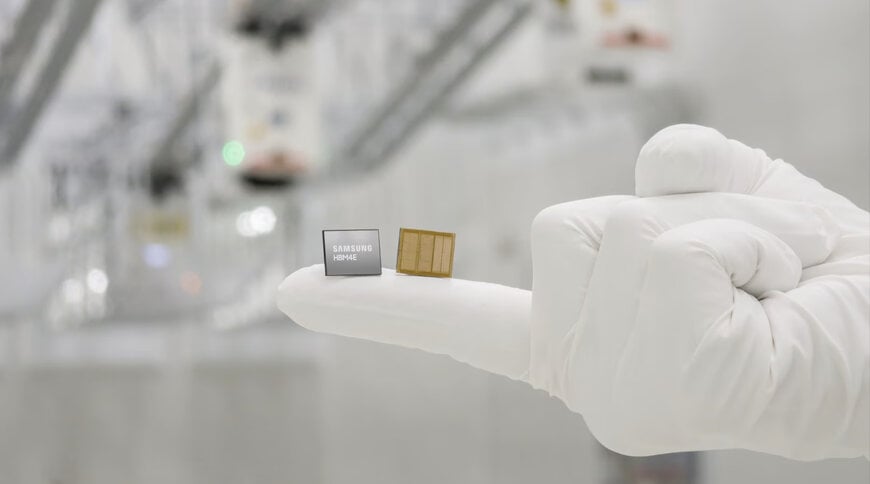
Samsung Electronics has started shipping samples of its 12-layer HBM4E high-bandwidth memory to major global customers, extending its roadmap for AI memory and hyperscale computing infrastructure. The new HBM4E platform increases memory bandwidth, storage density and thermal efficiency compared with the company’s previous HBM4 generation, addressing growing requirements from large language models, AI accelerators and next-generation data centers.
The announcement follows Samsung’s earlier mass production and commercial deployment of HBM4 memory earlier in 2026. With HBM4E, the company is targeting increasingly demanding AI workloads that require higher memory throughput, lower energy consumption and improved thermal management.
12-layer HBM architecture increases bandwidth and memory density
Samsung’s HBM4E is offered initially in a 12-layer configuration with a capacity of 48 GB per stack. According to the company, this represents more than a 30% increase in capacity compared with the previous generation. Additional versions are planned, including 32 GB eight-layer and 64 GB sixteen-layer configurations.
The memory delivers stable pin speeds of 14 Gbps, scalable up to 16 Gbps depending on system implementation. Samsung states that this represents more than a 20% performance increase over its HBM4 platform. Total memory bandwidth reaches up to 3.6 TB/s per stack, supporting the data-processing requirements of large language models, AI training systems and high-performance computing workloads.
High-bandwidth memory technologies are increasingly used alongside AI accelerators and graphics processors because they provide substantially higher data throughput than conventional server DRAM while minimizing latency between memory and compute resources.
Advanced DRAM and foundry technologies support manufacturability
The HBM4E platform combines Samsung’s sixth-generation 10 nm-class DRAM process technology, referred to as 1c DRAM, with a 4 nm logic base die manufactured through Samsung Foundry. The company indicates that this combination improves process stability, manufacturability and yield performance.
The architecture builds upon technologies previously developed for Samsung’s HBM4 production platform, allowing design and manufacturing optimizations across both memory and logic layers.
According to Samsung, coordinated optimization of the memory stack, base die architecture and packaging structure contributes to improved operational efficiency and thermal performance while supporting higher bandwidth requirements for AI systems.
Energy efficiency and thermal performance for AI data centers
Samsung reports that advanced low-power design techniques and packaging improvements increase energy efficiency by 16% compared with the previous generation. Thermal resistance characteristics have also improved by more than 14%, enhancing heat dissipation during sustained AI processing workloads.
As AI training clusters continue to scale, thermal management has become a critical factor in data center design. High-bandwidth memory systems generate significant thermal loads because they operate at extremely high transfer rates while remaining physically close to AI processors.
The improved thermal characteristics of HBM4E are intended to support longer operational reliability, lower cooling requirements and reduced energy consumption in hyperscale computing environments.
HBM memory expands within AI semiconductor ecosystems
According to Sang Joon Hwang, Executive Vice President and Head of Memory Development at Samsung Electronics, the introduction of HBM4E demonstrates the company’s continued investment in advanced memory manufacturing and infrastructure expansion for AI markets.
Samsung plans to begin mass production of HBM4E following customer qualification and optimization processes. The company stated that customer feedback on its HBM4 platform has been positive, particularly regarding performance and energy efficiency. HBM4 entered mass production earlier in 2026 and achieved transfer speeds of 11.7 Gbps during system-in-package validation testing.
The company’s broader semiconductor portfolio spans memory, foundry manufacturing, logic design and advanced packaging technologies, enabling tighter integration between compute and memory architectures required for AI infrastructure.
Additional Context: This section details technical specifications and competitive benchmarking not included in the original product announcement
HBM4E belongs to the latest generation of high-bandwidth memory technologies developed for AI accelerators, GPUs and advanced data-center processors. The technology builds on stacked DRAM architectures connected through through-silicon vias (TSVs), allowing significantly higher bandwidth than conventional DDR memory systems.
Samsung’s HBM4E delivers up to 16 Gbps per pin and 3.6 TB/s bandwidth per stack, compared with approximately 11.7 Gbps and 3.3 TB/s for its earlier HBM4 platform. The 48 GB 12-layer configuration also increases memory density by more than 30% over previous-generation products.
Competing technologies include SK hynix HBM4E and Micron HBM4 platforms, which target AI accelerators from companies such as NVIDIA, AMD and Google. Benchmark comparisons in this segment typically focus on bandwidth per stack, transfer speed, memory density, thermal efficiency and power consumption.
According to Counterpoint Research data cited by industry reports, SK hynix held approximately 57% of the HBM market during late 2025, followed by Samsung with 22% and Micron with 21%. Samsung’s early shipment of HBM4E samples positions the company to compete more aggressively in future AI memory deployments.
The use of a 4 nm logic base die and advanced 1c DRAM process technology reflects a broader industry trend toward tighter integration between memory and logic functions. Future AI accelerators are expected to require even higher bandwidth memory systems as model sizes and computational complexity continue to increase across generative AI, inference acceleration and hyperscale cloud infrastructure.
Edited by Sucithra Mani, Induportals editor – adapted by AI.
www.semiconductor.samsung.com
